Switching Between Battery and
2009年04月23日 09:53 本站整理 作者:佚名 用戶評論()
關鍵字:
Portable equipment that can operate from a battery pack or an external power source (such as a wall-adapter or external supply) needs to be able to smoothly switch between the two power sources. This application note describes a circuit (Figure 1) that switches power sources with good efficiency and without switching noise.
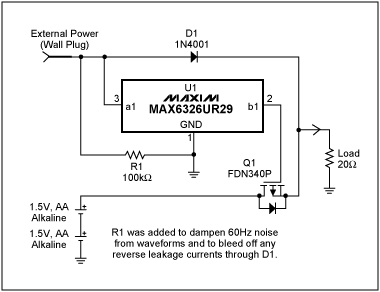
Figure 1. This circuit provides battery/wall-source switchover while debouncing the wall-source output.
Power Switching Problems
Two problems are addressed. First, contact bounce effects can occur when the external source is connected and disconnected, resulting in power spikes, as shown in Figure 2. Second, the switching method can introduce a voltage drop, reducing efficiency and battery life.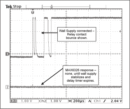
Figure 2. In Figure 1, the U1 output (bottom trace) remains unaffected as the wall-source voltage (top trace) is asserted.
Reducing Voltage Drop
A diode-OR connection is a common solution but the forward voltage drop of the diode limits efficiency. For a small battery pack of one to three cells, the voltage drop for a standard diode (0.6V to 0.7V) is a large percentage of the battery's terminal voltage. The use of a Schottky diode (0.3V to 0.5V drop) improves matters somewhat, but a FET switch can reduce the drop to less than 0.1V.The FET shown in Figure 1 was selected for its low Rds(on) and low Vgs, which is specified down to 1.8V. Thus, the FET can respond to a nearly discharged battery pack of two AA cells (0.9V each).
Reducing Switching Noise
The microprocessor-supervisory circuit (U1 in Figure 1) acts as a wall-source detector and debouncer. It monitors the wall supply and switches from battery power to the wall supply only when the wall supply is stable and has been at or above U1's trip voltage for a period of time. The battery will be back-driven (charged) during this delay period, which is typically 185mS. In Figure 1, note the effect on load voltage when switching from the battery to the wall supply (Figure 3) and vice versa (Figure 4).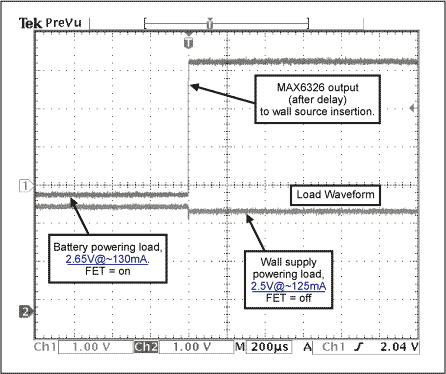
Figure 3. A 20Ω load in Figure 1 (bottom trace) registers a slight mismatch as the wall supply takes over from the battery, indicated (top trace) by the change in U1 output.
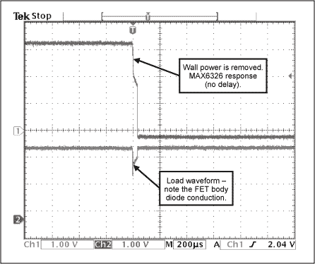
Figure 4. As wall power is removed in Figure 1 (indicated by U1's response in the top trace), the load response (bottom trace) shows the effect of a voltage drop across Q1's body diode.
U1's push-pull active-low output drives the gate of Q1 directly, without external components. If U1's time-out delay is too long, consider the pin-compatible MAX6801 (SOT23 package) or MAX6381 (SC70 package), which offer delay options of 1mS, 20mS, and higher. Another pin-compatible option is the MAX6375 voltage detector (SC-70 package). It provides no time-out delay, but incurs minimal back-drive effects on the battery.
Note that Q1 is reverse-connected with its drain to the battery and its source to the load, which allows its internal body diode to provide the initial current path to the load. At the same time, it blocks the wall supply from uncontrolled charging (back-driving) of the AA cells when Q1 is turned off.
A similar version of this article appeared in the May 13, 2002 issue of Electronic Design magazine.
非常好我支持^.^
(0) 0%
不好我反對
(0) 0%
相關閱讀:
- [新品快訊] Diodes推出PowerDI5封裝的超勢壘整流器(SBR)系列 2011-03-23
- [新品快訊] 新唐科技推出emPowerAudio系列ISD810X音頻功放 2011-03-22
- [電子動態(tài)] 2010年Digi-Key Corporation全球銷售額超越15億美元 2011-03-20
- [RF/無線] 突破單波長限制WDM-PON容量制勝 2011-03-16
- [廠商新聞] Silicon Labs看好中國EPON和嵌入式市場 2011-03-14
- [新品快訊] Excelsys推出1U模塊化電源開發(fā)套件powerKit 2011-03-10
- [新品快訊] 飛思卡爾提供針對工業(yè)市場的Power Architecture微控 2011-03-07
- [電源設計應用] MAX5981符合IEEE電源以太網(wǎng)標準(PoE)的系統(tǒng)接口 2011-03-03
( 發(fā)表人:發(fā)燒友 )