半導(dǎo)體切換開關(guān)-Semiconductor Toggle S
We are all used to single button on-off switches on portable appliances such as mobile (cellular) phones. The single button has several advantages over a toggling switch that delivers battery power directly to the electronics:
- It takes up less front panel space.
- It requires just one low-current, SPST, momentary-contact switch, which is typically more reliable, less expensive and requires simpler assembly.
- Power is delivered by circuitry rather than a pair of contacts that go straight to the battery. Protection can be provided against contact bounce and power glitches when batteries are inserted and removed, or when AC supplies are connected and disconnected.
- Orderly power-up and power-down sequences can be controlled by a microcontroller or other circuitry, which is has separate power available.
On products that include a microcontroller or microprocessor, this is normally implemented in a software routine. In simpler equipment, a latching circuit must be provided. This application note describes such a circuit.
The circuit below is a semiconductor toggle switch. The output state toggles in response to the pushbutton. It powers-up in a known state. It can directly drive a switched load or the enable or shutdown pins of a regulator (DC-DC converter or linear regulator).
The circuit is based on a MAX922, a dual comparator in an 8-pin package (DIL or surface-mount). The MAX922 is ideal for this application. It has a very low current consumption (2.5uA), wide supply range (2.5 to 11V), low input bias currents (10pA, allowing high impedance passive components) and its outputs can directly source loads up to 40mA.
The circuit is best explained by first ignoring C1 and C2.
Comparator A forms a latch. Comparator B is used to reinforce the drive to the latch input. This is weakly driven so it can be shifted by the push button.This drive is important - without it, the input could just float to a new value or the input would be open to stray signals and noise.
The RC network formed by R6 and C3 is used to store the current value of the latch built around comparator A. This is applied to the inverting input of the latch, causing it to change state. The voltage on C3 then changes slowly, preventing the switch from double-toggling in response to a single button press. Capacitor C2 in parallel with R5 is used to added protection against false triggering by external radiated noise by providing a lower impedance path for any high frequency signals. The capacitor is not connected to ground, as such a connection would upset the switching symmetry. Capacitor C1 is used to force the Latch State on power up, this circuit powers up with the output (pin 1) low. This state is also the lower power consumption state of the switch.
Most of the component values are not critical. None of the resistors need a precision tolerance. Capacitors C1 and C3 should be low-leakage components. Polyester film parts were used for the prototype. Capacitor C2 is not critical and a 100nF disk ceramic part was used. What is important with all the high impedance parts used is that the circuit board is clean and free from condensation. This circuit was prototyped on a plug-in circuit board with no leakage problems. If any debugging is done, awareness of the load that test equipment takes is important.
Both polarity outputs are available from pins 1 and 8 of the MAX922, which is especially handy for driving the enable or shutdown pins of linear regulators or DC-DC converters.
External circuits can control this latch if other functions are required. The best control point is pin 4 (the inverting input of comparator A). Diodes can be used to implement the pull up or pull down function.
This circuit was tested at 3V, 3.3V, 5V, 7V and 11V. If the circuit is only going to be used at 7V and 11V, then capacitor C2 should be increased in value.
The measured current consumption is shown below:
| Output Low | Output High | |
| 3V | 3.2uA | 4.5uA |
| 5V | 4.3uA | 6.6uA |
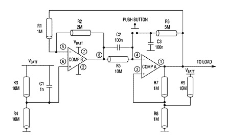
Figure 1.
非常好我支持^.^
(0) 0%
不好我反對
(0) 0%
相關(guān)閱讀:
- [消費類電子電路圖] 照明燈及溫度補償不受溫控開關(guān)控制電路 2011-03-26
- [新品快訊] MAX15041 內(nèi)置開關(guān)的同步DC-DC轉(zhuǎn)換器 2011-03-26
- [新品快訊] MAX16907 開關(guān)降壓轉(zhuǎn)換器 2011-03-26
- [新品快訊] MAX16909 集成高邊開關(guān)降壓轉(zhuǎn)換器 2011-03-26
- [新品快訊] MAX9132/MAX9134/MAX9135多輸入/輸出LVDS交叉開關(guān) 2011-03-25
- [開關(guān)電源] 開關(guān)電源設(shè)計中如何減小EMI 2011-03-24
- [新品快訊] Vishay推出用于3D快門式眼鏡的SPDT開關(guān)-DG9454 2011-03-24
- [新品快訊] 萊迪思半導(dǎo)體推出第三代LatticeECP3系列FPGA 2011-03-23
( 發(fā)表人:發(fā)燒友 )